Vertically Stacked GeSn Nanosheet pGAAFETs on Si by GeSn/Ge CVD Epitaxial Growth and Optimum Selective Etching
High-quality, fully compressively strained CVD-grown GeSn multi-layers are produced with defects confinement near the Ge buffer/Si interface. With the Ge layers used as sacrificial layers, the optimum ultrasonic-assisted H2O2 etching technique, the low thermal budget gate stack (400 °C), and the S/D parasitic resistance reduction, the first stacked 3-Ge0.93Sn0.07-nanosheets pGAAFET with LCH = 60 nm achieved record high Ion=1975μA/μm per channel width among all GeSn pFETs. Uniform stacked GeSn nanosheet GAAFETs with low surface roughness are compatible with Si technologies and are good candidates for future technology nodes to extend Moore’s law for CMOS scaling.

Related Publication:
- Yu-Shiang Huang, Fang-Liang Lu , Ya-Jui Tsou, Hung-Yu Ye, Shih-Ya Lin, Wen-Hung Huang, and C. W. Liu, ” Vertically Stacked Strained 3-GeSn-Nanosheet pGAAFETs on Si Using GeSn/Ge CVD Epitaxial Growth and the Optimum Selective Channel Release Process”, IEEE Electron Device Letters, Vol. 39, No. 9, pp.1274-1277, 2018.
- Yu-Shiang Huang, Fang-Liang Lu, Ya-Jui Tsou, Chung-En Tsai, Chung-Yi Lin, Chih-Hao Huang, and C. W. Liu, “First Vertically Stacked GeSn Nanowire pGAAFETs with Ion=1850μA/μm (VOV=VDS=-1V) on Si by GeSn/Ge CVD Epitaxial Growth and Optimum Selective Etching” International Electron Devices Meeting (IEDM), p832 ,2017.
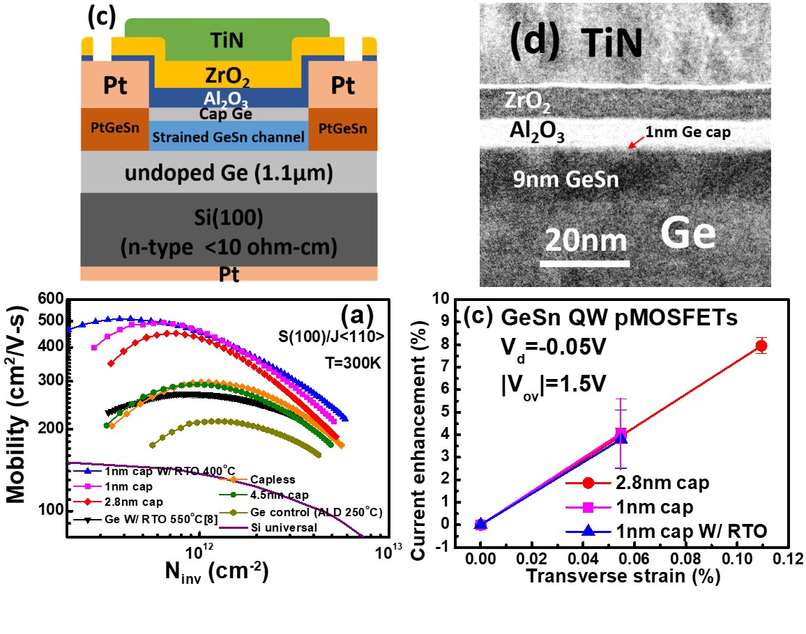
High Mobility CVD-grown Ge/Strained Ge0.9Sn0.1/Ge Quantum Well pMOSFETs on Si
The high peak mobility of 509 cm2/V-s of the CVD-grown GeSn pMOSFETs is obtained using 1nm Ge cap. The Ge cap on GeSn can reduce the scattering of oxide/interface charges and surface roughness for the holes in the GeSn quantum wells. However, the thick cap induces holes in the Ge cap itself, leading lower mobility than GeSn channels. The on current is enhanced by external stress due to the effective mass reduction.
Related Publication:
- Yu-Shiang Huang, Ya-Jui Tsou, Chih-Hsiung Huang, Chih-Hao Huang, Huang-Siang Lan, Chee Wee Liu, Yi-Chiau Huang, Hua Chung, Chorng-Ping Chang, Schubert S. Chu, and Satheesh Kuppurao., ” High-Mobility CVD-Grown Ge/Strained Ge9Sn0.1/Ge Quantum-Well pMOSFETs on Si by Optimizing Ge Cap Thickness”, IEEE Trans. on Electron Devices, Vol. 64, No. 6, pp.2498-2504, 2017.
- Yu-Shiang Huang, Chih-Hsiung Huang, Fang-Liang Lu, Chung-Yi Lin, Hung-Yu Ye,I-Hsieh Wong, Sun-Rong Jan, Huang-Siang Lan, C. W. Liu, Yi-Chiau Huang, Hua Chung, Chorng-Ping Chang, Schubert S. Chu, and Satheesh Kuppurao “Record High Mobility (428cm2/V-s) of CVD-grown Ge/Strained Ge0.91Sn0.09 /Ge Quantum Well p-MOSFETs,” International Electron Devices Meeting (IEDM), p822, 2016.
- Yu-Shiang Huang, Chih-Hao Huang, Chih-Hsiung Huang, Fang-Liang Lu, Da-Zhi Chang, Chung-Yi Lin, I-Hsieh Wong, Sun-Rong Jan, Huang-Siang Lan, W. Liu, Yi-Chiau Huang, Hua Chung, Chorng-Ping Chang, Schubert S. Chu, and Satheesh Kuppurao, “Strained Ge0.91Sn0.09 Quantum Well p-MOSFETs,” 22th IEEE Silicon Nanoelectronics Workshop (SNW), Honolulu, USA, June 12-13, 2016.
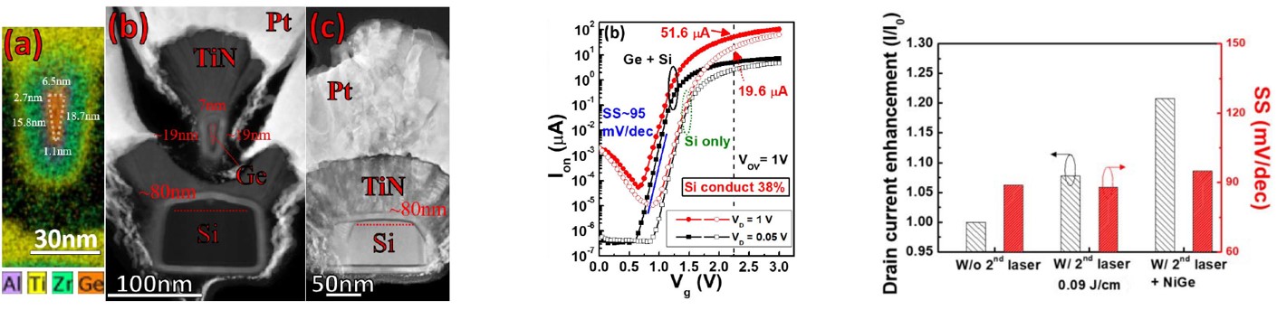
High Performance Ge Junctionless Gate-all-around NFETs using S/D Dopant Recovery by Selective Laser Annealing
The low channel doping concentrations of 1.2x1019 cm-3 to deplete the channel and the high S/D doping of 1.2x1020 cm-3 to reduce the S/D resistance are achieved simultaneously by selective laser annealing on the same CVD P-doped epi-Ge on SOI without ion implantation. The device with Wfin down to 7 nm, EOT = 2.2 nm, and Lch = 60 nm has Ion = 51.6 μA, Ion/Ioff = 2×10⁶, and SS = 95 mV/dec. The Ion can be further boost to 56 μA with external uniaxial tensile strain of 0.16%.
Related Publication:
- Fang-Liang Lu, Chung-En Tsai, I-Hsieh Wong, Chun-Ti Lu, and C. W. Liu Dopant Recovery in Epitaxial Ge on SOI by Laser Annealing With Device Applications IEEE Trans. on Electron Devices, Vol. 65, No. 7, pp.2925-2931, 2018.
- I-Hsieh Wong, Fang-Liang Lu, Shih-Hsien Huang, Hung-Yu Ye, Chun-Ti Lu, Jhih-Yang Yan, Yu-Cheng Shen, Yu-Jiun Peng, Huang-Siang Lan, and W. Liu, “High Performance Ge Junctionless Gate-all-around NFETs with Simultaneous Ion =1235 μA/μm at VOV=VDS=1V, SS=95 mV/dec, high Ion/Ioff=2E6, and Reduced Noise Power Density using S/D Dopant Recovery by Selective Laser Annealing,”International Electron Devices Meeting (IEDM), 2016.
- I-Hsieh Wong, Yen-Ting Chen, Shih-Hsien Huang, Wen-Hsien Tu, Yu-Sheng Chen, Tai-Cheng Shieh, Tzu-Yao Lin, Huang-Siang Lan, and C. W. Liu, “In-situ Doped and Tensily Stained Ge Junctionless Gate-all-around nFETs on SOI Featuring Ion = 828 uA/um, Ion/Ioff ~ 1E5, DIBL= 16-54 mV/V, and 1.4X External Strain Enhancement” p.239-242, International Electron Devices Meeting (IEDM), 2014.